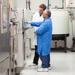
 For RF components to operate successfully in high-reliability Defense, Space, Oil and Gas, Automotive, and Medical applications it is imperative to identify any potential problems before releasing to market. To counter risk to reliable operation the semiconductor industry has developed a system by which early failures in components can be detected and then mitigated, burn-in testing.
What is burn-in testing for RF components?
 Burn-in testing can be best described as testing newly developed components to force failures to occur under managed conditions before being released to market. Ideally, any design defects or weak RF components would fail during this “burn-in” period so that they can be corrected, thus preventing a premature failure, infant mortality failure, or other defect at a later time. Specifically, burn-in testing is performed by applying thermal and electrical stresses to all of the components in a lot so that metallization, conductor, electromigration, and dielectric failures can be identified. For RF components, failures can be classified as random failures, wear-out failures, or early failures.
How is burn-in testing on RF components performed?
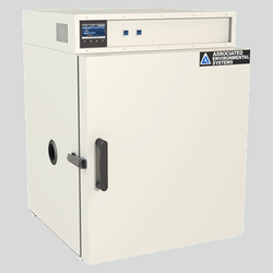
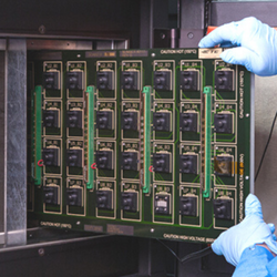
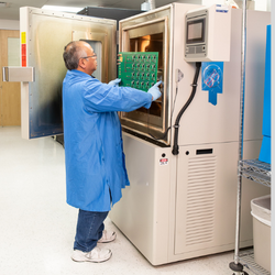
RF components are installed onto burn-in boards (BiBs), a printed circuit board (PCB) which acts as a jig. These burn-in boards are then loaded into burn-in chambers (BICs) where temperatures from 90 °C (194 °F) to 125 °C (257 °F) are applied to elevate the channel or junction temperatures. During burn-in, static or dynamic voltages are applied over an accelerated time frame. Typically, this time frame lasts from 48 to 300+ hours in length for component screening or 1,000 hours for High Temperature Operating Life (HTOL). As an example, the MIL-STD-883 Test method 1015.10 requires a minimum burn-in duration of 240 °C (464 °F) for Class S monolithic integrated circuits.
There are two main approaches to burn-in testing for RF components:
Static burn-in Test
During static burn-in, elevated temperatures at maximum voltages are applied to each RF component in the test sample.
Test approach factors to consider:
-
- A very simple and low-cost approach.
- No excitation inputs are applied to the components.
- The components are DC biased only with the inputs and outputs properly terminated.
- Unfortunately, this approach exercises less than 50% of the circuit nodes.
Dynamic burn-in Test
During dynamic burn-in, components are subjected to harsh temperatures and voltages while additional stresses, such as heightened frequency ranges, are applied.
Test approach factors to consider:
-
- The components are in an operational state.
- Inputs are applied to the components.
- The capability to administer stresses on internal circuits resulting in the identification of further failures.
- While this approach exercises more circuits within the device, it does not exercise 100% of all of the circuit nodes.
Conclusion
 There is no doubt that burn-in testing is a pillar for providing quality control to the many aspects of manufacturing RF components for high-reliability defense, space, oil and gas, commercial semiconductor, medical and automotive applications. Extensive engineering goes into burn-in testing, such as test program, socket and printed circuit board (PCB) design. Some companies outsource burn-in testing as it is challenging to develop proficiencies in all RF test disciplines. No matter the approach a company decides on, burn-in testing is essential to gauging and advancing RF component reliability.
Want to stay up-to-date on the latest content and news from Criteria Labs?
