The gettering process was initially developed during the era of glass vacuum tubes. Back then, components inside of these glass vacuum tubes were typically covered in a getter material, such nickel. When unwanted gas molecules and other impurities interacted with the getter material, they combined with it chemically or through absorption, resulting in reliable operation for the life of the vacuum tube. Fast forward to today and gettering is still a very important step in the pre-production device manufacturing process. Read on below to learn more.
What does gettering mean?
 Simply put, gettering is the means by which device-degrading impurities typically found in the active circuit regions of semiconductors are removed. While challenging, it is important to reduce the concentration of unwanted elements that impede RF device performance.
Example impurities include:
- Foreign metals
- Alkali ions
- H2O
There are two commonly accepted approaches to the gettering process- extrinsic and intrinsic gettering.
Why is gettering important?
 Semiconductor wafer materials are quite sensitive and require preparation prior to RF device manufacturing. While clean manufacturing and semiconductor cleaning processes are both effective methods in preventing contamination, gettering is an important secondary process that further aides in the removal of performance inhibiting elements.
H2O, foreign metals, and alkali ions are the primary causes of silicon wafer failure and can negatively impact conduction, putting RF device circuitry at significant risk. When silicon wafers are inconsistent in composition defects are likely to occur, the end result being RF device failure. The gettering process is also beneficial in that it neutralizes foreign gases that are typically found in semiconductor wafer material.
Having a clean and contaminate free silicon wafer will determine whether or not your RF device will operate to desired specifications. Cutting to the chase, it is important to include gettering as a required step in the pre-production device manufacturing process.
What is extrinsic gettering?
 Extrinsic gettering is a process that involves applying stresses such abrasion and grooving to the silicon wafer itself. The applied stress creates dislocations where impurities can then be trapped or chemically neutralized. This process typically occurs on the reverse side of the silicon wafer.
While extrinsic gettering is a very effective process it does have its limitations. One example being poor stability when conducted at higher temperatures (1200 ºC+).
What is intrinsic gettering?

Intrinsic gettering is a process by which supersaturated oxygen is precipitated out of the silicon wafer. Unlike extrinsic gettering this process has a distinct advantage in that the only stress applied is heat. The applied thermal stress causes clusters to develop and grow on the bulk regions of the wafer, resulting in dislocations or faults being formed. Clusters can be prevented from forming near the active device areas of a silicon wafer by limiting the concentration of oxygen levels beneath the minimum precipitation levels. The resulting dislocation and fault sites trap impurities.
Our Gettering Approach and RF Device Manufacturing Solutions
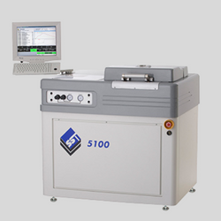 Criteria Labs utilizes state of the art vacuum sealing and solder reflow furnaces with getter firing capabilities to effectively remove performance inhibiting impurities prior to RF device manufacturing. Our vacuum sealing and solder reflow furnaces create void-free, flux-free solder joints ideal for operation in high-reliability aerospace and harsh environment applications.
With broad in-house capabilities, our engineering and manufacturing teams provide end-to-end RF engineering solutions for high-reliability aerospace, defense, commercial semiconductor, automotive, and medical applications. Based on your unique requirements, Criteria Labs can determine the optimum RF device manufacturing process, and procure all of the required materials for assembly in a class 100 clean room.
Want to stay up-to-date on the latest content and news from Criteria Labs?
